![]() CG - Chinese Group
CG - Chinese Group
In this proposal we will develop a novel fabrication approach by utilizing colloidal nanoparticles as a lithographic mask and characterize the properties in the In-situ measurement system.
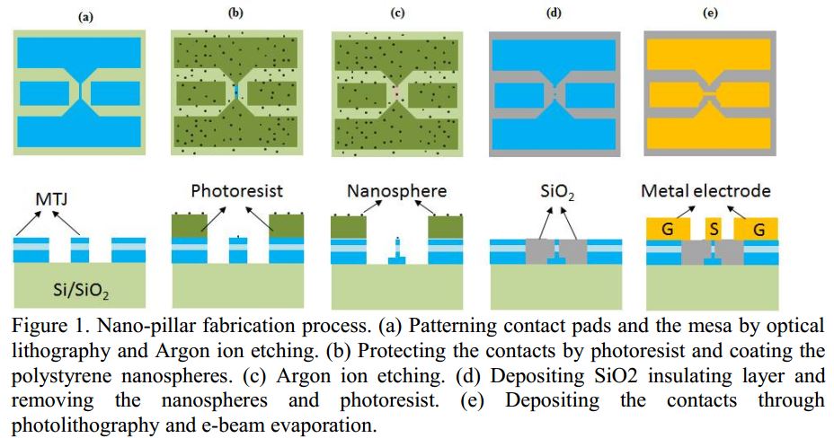
The fabrication process is described as follows. Firstly, standard photolithography and Ar ion milling were used to pattern the contact pads and the 6×50 μm2 mesas as shown in Fig. 1(a). Then the second photolithography step was introduced to open a window that allows the polystyrene nanopheres to adhere to the top of the mesas. The photoresist was also used to
protect the contact pads from the nanopheres and SiO2 insulator deposition. The next step is a key part of the fabrication process that defines the MTJ nanopillars by colloidal lithography. The nanospheres with a diameter of 160 nm was uspended in a deionized (DI)-based solvent by ultrasound 3 minutes in order to improve dispersity. Before coating spheres, the wafer was coated with hexamethyldisilazane (HMDS) that strengthens adhesion between wafer and nanospheres, the spheres was spin-coated on the surface to act as etching mask for subsequent etching (Fig. 1(b)). After that the Argon ion milling was used to etch the materials without protection by photoresist and nanospheres (Fig. 1(c)). This was followed by depositing a 50 nm SiO2 insulator layer by Inductively-Coupled-Plasma CVD (ICP-CVD) system at low temperature (~ 75 °C). Next, the wafer was dipped in dichloromethane and resist-remover to remove the spheres as well as the photoresist (Fig. 1(d)). The fabrication of devices is completed by contacting the nanopillars and the two ground contacts to form a Ti (10 nm)/Au (100 nm) ground-signal-ground (GSG) waveguide, deposited using electron beam evaporation and patterned using optical lithography and lift off (Fig. 1(e)).